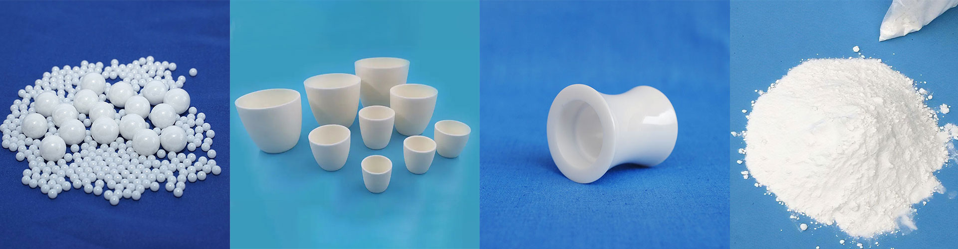


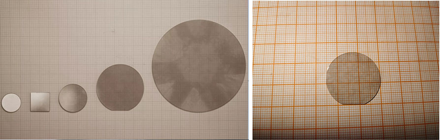
AIN Single Crystal Substrate has the advantages of a wide bandgap, high breakdown electric field, high thermal conductivity, high electron saturation rate, and high radiation resistance. Nextgen Advanced Materials supplies AlN Single Crystal Substrate with high-quality and competitive price. With our strong R&D and manufacturing capability, we can do customization.
You can rest assured to buy customized Nextgen AIN Single Crystal Substrate from us. AlN single crystal substrate is a wide bandgap semiconductor material with exceptional characteristics.
The band gap is 6.2eV and has a direct band gap. It is an important blue and ultraviolet light-emitting material with high thermal conductivity, high melting point, high resistivity, strong breakdown field and low dielectric coefficient. It is an excellent electronic material for high temperature, high frequency and high-power devices.
| Item | TGS-AlN-025B |
| Size (mm) | 25.4 ± 0.5 |
| Thickness (μm) | 400 ± 50 |
| Crystal form | 2H |
| Crystal direction | {0001} ± 0.5 ° |
| Surface polishing | aluminum surface: chemical polishing |
| RMS (nm) | Roughness of aluminum surface: ≤ 0.5nm |
| RMS (nm) | Nitrogen side (back): ≤ 1.2um |
| Shape | Circular shape with locating edge |
| Quality grade | P (production) |
| HRXRD FWHM @(0002) (arcsec) | ≤300 |
| HRXRD FWHM @(10-02) (arcsec) | ≤200 |
| absorption coefficient | ≤70 |
| @265nm (cm-1) | |
| Edge removal area (mm) | 1 |
| Scratch | free |
| Collapse edge | none |
| Usable area | ≥80% |
| Main positioning edge orientation | {10-10} ± 5.0° |
| Orientation of secondary positioning | surface to aluminum: surface: rotate 90 ° ± 5 ° clockwise along the direction of main |
| positioning edge | |
| Nitrogen side: rotate 90 ° ± 5 ° anticlockwise along the direction of the main positioning edge | |
| TTV (μm) | ≤ 30 |
| Warpage (µ m) | ≤ 30 |
| BOW (μm) | ≤ 30 |
| Crack | The crack is located at the edge of the wafer and < 1mm |
| Hexagonal hole | size<300um, and number ≤ 2 |