
Ion implantation equipment operates at the intersection of high voltage, high vacuum, corrosive process gas, and plasma. The beamline must accelerate ions to precise energies, the wafer chamber must remain ultraclean, and the insulating structures must survive electrical stress without tracking, outgassing, or particulate generation. Alumina Ceramic, a high-purity aluminum oxide material, is one of the few materials that can meet all of these requirements at once. It provides dielectric strength, mechanical rigidity, thermal stability, and plasma resistance in a single machinable format. For a procurement team sourcing components for ion implantation tools, understanding the role of Alumina Ceramic is the first step in qualifying a material that will not become the weak link in the beamline.
This guide is written for buyers and engineers who specify ceramic components for semiconductor capital equipment. It explains why the ion implantation environment demands a high-performance insulator, which components typically use Alumina Ceramic, how the material resists plasma and corrosive gas attack, which specifications should be verified before an order is placed, and how the material compares with alternative ceramics and polymers. The content is organized around the questions a procurement team should ask, and it includes the product parameters and test documentation that a reliable supplier should provide. Nextgen Advanced Materials INC supplies technical ceramics for semiconductor equipment, and the guidance below reflects the engineering and sourcing standards applied to the materials supplied to our customers.
The ion implantation environment is unusually demanding for insulating materials because several stressors act at the same time. The extraction electrode and the beamline operate at high voltage, often in the tens of kilovolts and sometimes higher. The insulating structures that support the electrodes must withstand the voltage without surface tracking or bulk breakdown. The chamber is held at high vacuum, so the material must have low outgassing and low porosity. The process gas may include boron trifluoride, phosphine, arsine, or other corrosive species. The plasma generates ultraviolet radiation and energetic ions that can erode organic materials and degrade polymers. The wafer environment also demands low particle generation and low metallic contamination.
A material that satisfies only one of these requirements is not sufficient. A polymer with high dielectric strength may outgas in vacuum or erode in plasma. A metal with high strength may conduct current or contaminate the wafer. A lower-grade ceramic may have porosity that traps moisture and causes electrical tracking. The table below maps the operating stressors to the material requirements that follow from them.
| Operating Stressor | Material Requirement | Consequence of Non-Compliance |
| High voltage | High dielectric strength, high volume resistivity | Surface tracking, flashover, equipment downtime |
| High vacuum | Low outgassing, low porosity, high purity | Vacuum contamination, extended pump-down time |
| Corrosive gas | Chemical inertness, corrosion resistance | Surface erosion, particle generation, leakage |
| Plasma exposure | Plasma resistance, low sputter yield | Component wear, metallic contamination |
| Thermal cycling | Low thermal expansion, thermal shock resistance | Cracking, loss of dimensional stability |
| Wafer cleanliness | Low particle shedding, low metallic content | Defectivity, yield loss |
Alumina Ceramic is attractive because it addresses all six stressors in one material family. It has a dielectric strength that is high enough for the extraction and beamline insulation, a volume resistivity that remains high at elevated temperature, a purity level that can be controlled to the 99.5 percent to 99.9 percent range, and a chemical inertness that resists the process gases. The material is also machinable to the tolerances required for vacuum seals and electrode supports. These properties are the reason Alumina Ceramic has become a standard material in ion implantation equipment.
The procurement implication is that the material should be specified by the property set, not by the generic name. Two suppliers may offer “alumina” with different purity, density, and surface finish, and the difference can determine whether the component performs in the tool. Nextgen Advanced Materials INC supports customers by providing the property data and the process controls that allow the material to be matched to the specific location in the ion implantation equipment.
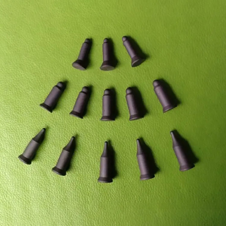
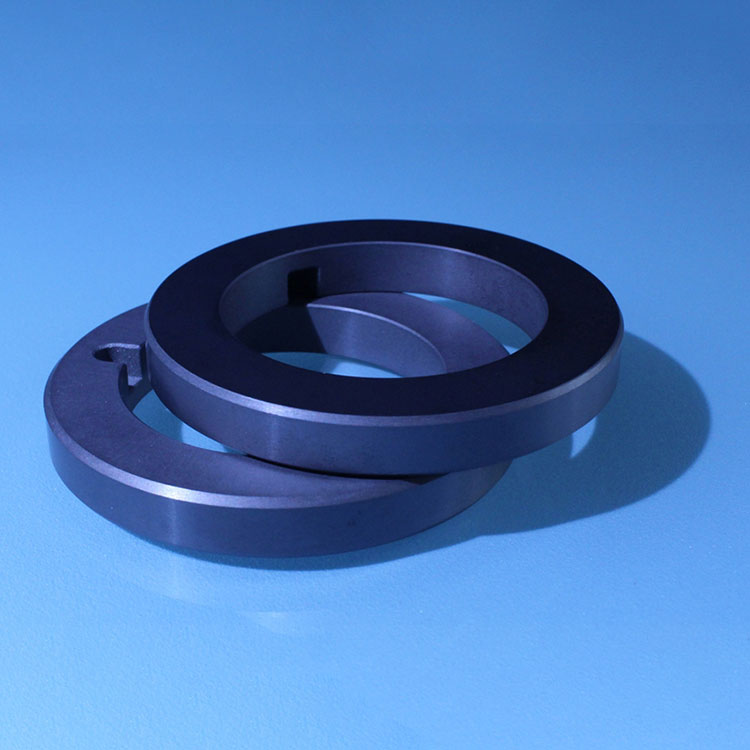
Alumina Ceramic appears in several locations in an ion implantation tool, and each location has a different functional requirement. The high-voltage insulator is the most visible application. It supports the extraction electrode and isolates the high-voltage assembly from the grounded chamber. The insulator must be designed with a profile that controls the electric field and reduces the risk of surface tracking. The gas feedthrough insulator is another application. It isolates the gas line from the high-voltage components and must be leak-tight against the process gas. The wafer handling components, such as end effectors and support pins, use alumina because it is dimensionally stable and does not shed particles. The plasma chamber liners and shields use alumina because it resists erosion and does not introduce metallic contamination. The table below lists the common components and their functional requirements.
| Component | Function | Key Material Requirement | Procurement Focus |
| High-voltage insulator | Isolates extraction electrode from ground | Dielectric strength, tracking resistance | Purity, surface finish, profile |
| Gas feedthrough insulator | Isolates gas line and seals vacuum | Gas tightness, corrosion resistance | Porosity, seal design, leak rate |
| Wafer support pins | Supports wafer during handling | Dimensional stability, low particle shedding | Tolerance, surface roughness, cleanliness |
| Plasma chamber liner | Protects chamber wall from plasma | Plasma resistance, low sputter yield | Purity, density, erosion rate |
| Beamline spacer | Maintains electrode spacing | Mechanical strength, thermal stability | Strength, thermal expansion, flatness |
| RF window | Transmits RF power into the plasma | Low dielectric loss, vacuum tightness | Loss tangent, dielectric constant, seal |
The component list shows that Alumina Ceramic is not used as a generic substitute for metal or plastic. It is selected because the component sits in a location where electrical, chemical, and mechanical requirements intersect. The high-voltage insulator is a good example. The insulator must be thick enough to withstand the voltage, but thin enough to fit the available space. It must have a profile that controls the electric field, but it must also be manufacturable at a reasonable cost. The surface finish must be smooth enough to resist tracking, but rough enough to allow a reliable bond if a coating is applied. These trade-offs are the reason the component should be specified with the supplier, not selected from a catalogue.
Nextgen Advanced Materials INC works with equipment engineers to define the geometry, the surface finish, and the purity level for each component. Our factory can produce insulators, spacers, liners, and handling components in high-purity Alumina Ceramic, and we can provide the dimensional and electrical test data for each production lot. The goal is to supply a component that fits the location, not just a material that meets a generic specification.
Alumina Ceramic withstands plasma and corrosive gas attack because its surface chemistry is stable under the conditions that degrade polymers and etch metals. The material is an oxide ceramic, and its surface is already in an oxidized state. It does not have the carbon backbone that makes polymers vulnerable to plasma erosion, and it does not have the free metal that makes metals susceptible to corrosion and contamination. The plasma resistance of alumina depends on its purity, its density, and its grain boundary chemistry. A high-purity alumina with a dense microstructure has fewer grain boundaries and fewer impurities, so it erodes more slowly and releases fewer particles. The table below summarizes the degradation mechanisms and the material properties that resist them.
| Degradation Mechanism | Effect on the Material | Resistance Property | Procurement Evidence |
| Ion bombardment | Physical sputtering of the surface | Low sputter yield, high hardness | Erosion rate data |
| Chemical etching | Attack by fluorine or chlorine species | Chemical inertness, low impurity content | Corrosion test data |
| Thermal shock | Cracking from rapid temperature change | Low thermal expansion, high strength | Thermal cycling test data |
| Particle generation | Debris that contaminates the wafer | High density, fine grain structure | Particle count and microstructure data |
| Outgassing | Contamination of the vacuum environment | Low porosity, high purity | Outgassing test data |
The practical implication is that the plasma resistance of Alumina Ceramic is not a single number. It depends on the grade, the manufacturing process, and the surface condition. A 99.5 percent alumina with a porosity of several percent will erode faster and generate more particles than a 99.9 percent alumina with a near-theoretical density. The buyer should request the erosion rate, the particle count, and the microstructure data for the specific grade, not assume that all alumina behaves the same way.
Nextgen Advanced Materials INC controls the purity, the density, and the grain size of our Alumina Ceramic components, and we test the plasma erosion rate on representative samples. Our factory also offers surface treatments that can further reduce particle generation in sensitive locations. The goal is to provide a component that resists the plasma environment for the expected service interval, not just a material that is labeled as alumina.
The specifications that matter for ion implantation are purity, density, dielectric strength, volume resistivity, thermal expansion, thermal conductivity, flexural strength, hardness, surface roughness, dimensional tolerance, gas tightness, and outgassing. Each specification should be matched to the location in the tool. A high-voltage insulator may prioritize dielectric strength and tracking resistance, while a wafer support pin may prioritize dimensional stability and particle shedding. The table below presents the typical specification range for high-purity Alumina Ceramic used in ion implantation equipment.
| Parameter | Typical Range | Why It Matters in Ion Implantation | Verification Method |
| Purity | 99.5 percent to 99.9 percent | Reduces metallic contamination and improves plasma resistance | Chemical analysis certificate |
| Density | 3.85 to 3.95 grams per cubic centimeter | Higher density reduces porosity and particle generation | Archimedes density test |
| Dielectric strength | 15 to 20 kilovolts per millimeter | Prevents breakdown in high-voltage insulators | Dielectric breakdown test |
| Volume resistivity | Greater than 10 to the 14 ohm-centimeter | Prevents leakage current at elevated temperature | Resistivity test at temperature |
| Thermal expansion | 7.5 to 8.5 parts per million per degree C | Matches adjacent materials and reduces thermal stress | Dilatometer test |
| Thermal conductivity | 20 to 30 watts per meter kelvin | Helps dissipate heat from the beamline components | Laser flash test |
| Flexural strength | 300 to 400 megapascals | Supports mechanical loads without fracture | Four-point bend test |
| Hardness | 1500 to 1800 HV | Resists wear and erosion | Vickers hardness test |
| Surface roughness | 0.2 to 0.8 micrometer Ra | Controls particle adhesion and tracking resistance | Profilometer measurement |
| Dimensional tolerance | Plus or minus 0.01 to 0.05 millimeter | Ensures fit and alignment in the assembly | Coordinate measuring machine |
| Gas tightness | Leak rate below 1 times 10 to the minus 9 mbar liter per second | Prevents vacuum loss and process gas leakage | Helium leak test |
| Outgassing | Low, with no significant hydrocarbon release | Protects vacuum quality and wafer cleanliness | Outgassing test per ASTM E595 |
The table is a starting point for the specification review. The actual requirements depend on the component and the tool design. The buyer should confirm the specification with the equipment engineer and should request the test data for the production lot. A supplier that provides only a generic datasheet is a supplier that is not demonstrating control of the specific component. Nextgen Advanced Materials INC provides lot-specific test data for purity, density, dielectric strength, and dimensional tolerance, and our factory can perform helium leak testing and outgassing testing on request.
The specification review should also include the surface finish and the edge quality. A sharp edge on a ceramic component can concentrate the electric field and initiate a tracking path. A rough surface can trap particles and moisture. A chamfer or a radius on the edge is often specified to reduce the field enhancement. These details are not captured by the bulk material specification, but they are part of the component specification that determines performance.
Alumina Ceramic is not the only material available for ion implantation components, and the comparison with other ceramics and polymers helps explain why it is so widely used. The main alternatives are aluminum nitride, silicon nitride, silicon carbide, zirconia, PEEK, PTFE, and polyimide. Each has a different balance of dielectric strength, thermal conductivity, plasma resistance, machinability, and cost. The comparison below is framed for procurement decisions rather than material science.
| Material | Dielectric Strength | Thermal Conductivity | Plasma Resistance | Machinability | Typical Limitation |
| Alumina Ceramic | High | Moderate | Good | Good | Moderate thermal conductivity |
| Aluminum nitride | High | Very high | Good | Moderate | Higher cost, moisture sensitivity |
| Silicon nitride | High | Moderate | Very good | Moderate | Higher cost, limited suppliers |
| Silicon carbide | Moderate | High | Good | Difficult | Conductive in some grades |
| Zirconia | Moderate | Low | Moderate | Good | Higher density, lower thermal shock resistance |
| PEEK | Moderate | Low | Poor | Excellent | Outgassing, plasma erosion |
| PTFE | Moderate | Low | Poor | Excellent | Cold flow, particle generation |
| Polyimide | Moderate | Low | Moderate | Excellent | Moisture absorption, outgassing |
The comparison shows that Alumina Ceramic is a balanced choice. It does not have the highest thermal conductivity, which is why aluminum nitride is used in some heat-sensitive locations. It does not have the highest plasma resistance, which is why silicon nitride and silicon carbide are used in some extreme environments. It does not have the machinability of PEEK or PTFE, which is why polymers are used in some non-critical locations. But it combines high dielectric strength, good plasma resistance, good machinability, and moderate cost in a way that fits most ion implantation components. This balance is the reason Alumina Ceramic has become the default material for high-voltage insulators and beamline spacers.
For a buyer, the comparison should be used to confirm that the material choice is justified for the specific component. If the component is a high-voltage insulator, alumina is likely the correct choice. If the component is a thermal spreader, aluminum nitride may be better. If the component is a low-cost shield in a non-critical location, a polymer may be acceptable. The procurement team should ask the supplier to explain the material selection for each component, not just provide a catalogue of available materials.
Nextgen Advanced Materials INC supplies Alumina Ceramic components for ion implantation equipment and can support the material selection with property data and application experience. Our factory can also provide alternative ceramic materials when the application requires a different balance of properties. The goal is to help the buyer select the material that fits the component, not to force every component into the same material.
Question 1: What purity of alumina ceramic is suitable for ion implantation insulators?
Answer: High-voltage insulators in ion implantation equipment typically use 99.5 percent to 99.9 percent purity alumina. The higher purity reduces metallic contamination and improves plasma resistance. The exact purity should be matched to the component location and the tool cleanliness requirement. The buyer should request the chemical analysis certificate for the production lot and confirm that the purity is consistent with the specification.
Question 2: Why does alumina ceramic need a smooth surface finish for vacuum components?
Answer: A smooth surface finish reduces particle adhesion, improves cleanability, and lowers the risk of surface tracking in high-voltage applications. A rough surface can trap moisture and particles, which can lead to electrical leakage or contamination. Typical surface roughness for vacuum components is 0.2 to 0.8 micrometer Ra, depending on the component and the cleaning process.
Question 3: Can alumina ceramic be machined to the tolerances required for ion implantation components?
Answer: Yes, high-purity alumina can be machined to tolerances of plus or minus 0.01 to 0.05 millimeter, depending on the feature and the component size. Diamond grinding is typically used for the final dimensions and the surface finish. The buyer should confirm the tolerance and the measurement method with the supplier, and should request the dimensional inspection report for the production lot.
Question 4: How does alumina ceramic compare with aluminum nitride for ion implantation?
Answer: Alumina ceramic has higher dielectric strength and better availability at a lower cost, while aluminum nitride has much higher thermal conductivity. Aluminum nitride is used in heat-sensitive locations where the heat must be spread or conducted away. Alumina is used in high-voltage insulation and structural components where the thermal load is moderate. The choice depends on the component function, not on a general preference.
Question 5: What documentation should accompany an alumina ceramic component order for semiconductor equipment?
Answer: The documentation should include the chemical analysis certificate, the density and porosity data, the dielectric strength and volume resistivity data, the dimensional inspection report, the surface roughness measurement, and the cleanliness and outgassing data where applicable. For vacuum components, a helium leak test report should also be provided. The documentation allows the buyer to verify that the component meets the specification for the specific location in the ion implantation equipment.
Alumina Ceramic plays a critical role in ion implantation equipment because it combines high dielectric strength, vacuum compatibility, plasma resistance, and dimensional stability in a single material. It is used in high-voltage insulators, gas feedthroughs, wafer support components, plasma chamber liners, and beamline spacers, where the electrical, chemical, and mechanical requirements intersect. The material is not a commodity, and the specification should be verified by purity, density, dielectric strength, thermal properties, surface finish, and dimensional tolerance. For procurement teams, the key is to specify the component by the property set and the location, and to request the lot-specific test data before the order is placed. Nextgen Advanced Materials INC supplies Alumina Ceramic components for semiconductor equipment and supports customers with material data, component design, and production testing. If you are sourcing ceramic components for ion implantation equipment, contact our team to discuss the specification and the verification data for your application.
Contact Nextgen Advanced Materials INC today to discuss your Alumina Ceramic requirements for ion implantation equipment and to request the material and component test documentation for your application.